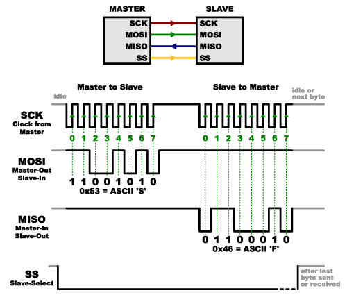
The SPI is a high-speed synchronous serial input/output port that allows a serial bit stream of programmed length (2 to 16 bits) to be shifted into and out of the device at a programmed bit-transfer rate. The SPI is normally used for communication between the device and external peripherals. Typical applications include interface to external I/O or peripheral expansion via devices such as shift registers, display drivers, SPI EPROMS, and analog-to-digital converters.
The SPI has the following features: • 16-bit shift register • 16-bit Receive buffer register (SPIBUF) and 16-bit Receive buffer emulation alias register (SPIEMU) • 16-bit Transmit data register (SPIDAT0) and 16-bit Transmit data and format selection register (SPIDAT1) • 8-bit baud clock generator • Serial clock (SPICLK) I/O pin • Slave in, master out (SPISIMO) I/O pin • Slave out, master in (SPISOMI) I/O pin • Multiple slave chip select (SPISCS[n]) I/O pins (4 pin mode only) • Programmable SPI clock frequency range • Programmable character length (2 to 16 bits) • Programmable clock phase (delay or no delay) • Programmable clock polarity (high or low) • Interrupt capability • DMA support (read/write synchronization events) • Up to 66 MHz operation
The SPI allows software to program the following options: • SPICLK frequency (SPI module clock/2 through SPI module clock/256) • 3-pin and 4-pin options • Character length (2 to 16 bits) and shift direction (MSB/LSB first) • Clock phase (delay or no delay) and polarity (high or low) • Delay between transmissions in master mode. • Chip select setup and hold times in master mode • Chip select hold in master mode
The SPI does not support the following features: • Multibuffer mode • Parallel mode or parity • SPIENA pin • SPI slave mode • GPIO mode
How it works:
The SPI operates in master mode. The SPI bus master is the device that drives the SPICLK, SPISIMO, and optionally the SPISCS[n] signals, and therefore initiates SPI bus transfers. The CLKMOD and MASTER bits in the SPI global control register 1 (SPIGCR1) selects master mode. In the master mode, the SPI supports two options: • 3-pin option • 4-pin with chip select option The 3-pin option is the basic clock, data in, and data out SPI interface and uses the SPICLK, SPISIMO, and SPISOMI pins. The 4-pin with chip select option adds the SPISCS[n] pin that is used to support multiple SPI slave devices on a single SPI bus.
The SPI in master mode supports several options to modify the timing of its generation of the chip select signal (SPISCS[n]). This allows the SPI to support the timing requirements of various slave devices without adding additional overhead to the CPU by generating the appropriate delays automatically.
Chip Select Setup Time:
The master can be configured to provide a (slow) slave device a certain chip select setup time to the first edge on SPICLK. This delay is controlled by the C2TDELAY field in the SPI delay register (SPIDELAY) and can be configured between 2 and 257 SPI module clock cycles. The C2TDELAY is applicable only in 4-pin with chip select mode. The C2TDELAY begins when the SPI master asserts SPISCS[n]. The C2T delay period is specified by:
Maximum duration of C2TDELAY period = SPIDELAY.C2TDELAY + 2 (SPI module clock cycles)
The previous value of the CSHOLD bit in the SPI transmit data register (SPIDAT1) must be cleared to 0 for the C2T delay to be enabled.
Chip Select Hold Time:
The master can be configured to provide a (slow) slave device a certain chip select hold time after the last edge on SPICLK. This delay is controlled by the T2CDELAY bit in the SPI delay register (SPIDELAY) and can be configured between for 1 and 256 SPI module clock cycles. The T2CDELAY is applicable only in 4-pin with chip select mode. The T2CDELAY begins after the data shifting period ends. The T2C delay period is specified by:
Maximum duration of T2CDELAY period = SPIDELAY.T2CDELAY + 1 (SPI module clock cycle) If the PHASE bit in the SPI data format register n (SPIFMTn) is 0, then the T2CDELAY period lasts for an additional ½ SPICLK time over that specified by the above equation.
The current value of the CSHOLD bit in the SPI transmit data register (SPIDAT1) must be cleared to 0 for T2C delay to be enabled.
The programmable configuration capability of the SPI allows it to gluelessly interface to a variety of SPI format devices. The SPI does not conform to a specific industry standard.